 English
 हिन्दी
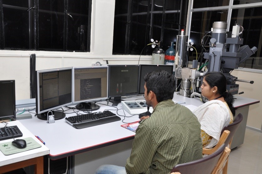
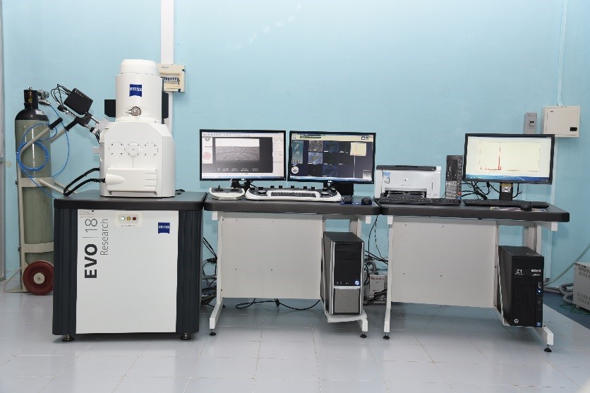
Scanning Electron Microscope (SEM)
Image formation in an SEM is accomplished through collection of the secondary electrons / back scattered electrons generated due to interaction of an electron beam with the material of the specimens. The characteristic X-rays generated from the specimens during this interaction are used for elemental analysis.
|
Equipment Details |
Key Features |
Application Areas |
|
Model:EVO 18 Research Manufacturer:Carl Zeiss, UK Resolution:15 nm in SE mode Operating Parameters:0.2 to 30 kV accelerating voltage and 0.5 pA to 5 µA probe current |
|
|