 English
 हिन्दी
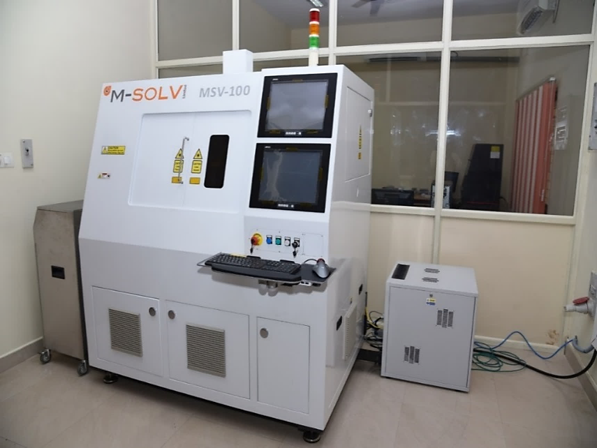
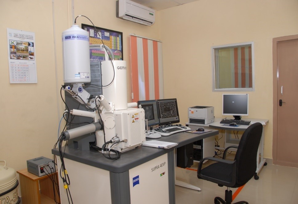
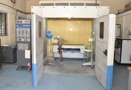
Laser Micromachining Facility for Ceramic Substrates
In recent years, there is a growing demand for laser micromachining of structural and electronic ceramics for different applications such as microelectronics, space electronics, sensors, fuel cells, etc. Laser machining is a prospective, rapid, non-contact and flexible technique for micromachining of ceramics as brittle and hard ceramics can be machined with ease and materials can be removed at a higher rate. The Laser Micromachining Facility at SED is a custom-built machine consisting of two lasers integrated on a single high precision stage. The quasi-continuous wave (QCW) ytterbium fiber laser (wavelength = 1070 nm) can deliver a peak power of 1500 W in pulsed mode, 250 W in continuous mode and 150 W in quasi-continuous mode and can be used for precise drilling, scribing and cutting of sintered ceramics. The nanosecond pulsed green fiber laser (wavelength = 532 nm) can operate with a nominal average power of 20 W and can be used for machining of green ceramic substrates. The machine is capable of machining both green and sintered ceramic substrates and can be used for cutting and shaping of both green and sintered ceramics such as alumina, zirconia, aluminium nitride, NiO-YSZ, etc. It can also find application in wafer downsizing of most semiconductor materials, high speed via drilling in ceramics and semiconductor materials, scribing, marking and etching of ceramics. This facility can also be customized for machining aerospace alloys.
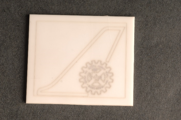
Laser engraved CSIR-NAL logo on alumina ceramic substrate