Piezoceramic thin films and coatings
Conformal Piezoceramic coating on Aerospace Grade Aluminum metal, Composite Structures and Silicon wafer has been successfully developed in the Materials Science Division (MSD) of CSIR - National Aerospace Laboratories to fabricate insitu sensors, actuators and MEMS devices.
Brief description of the technique
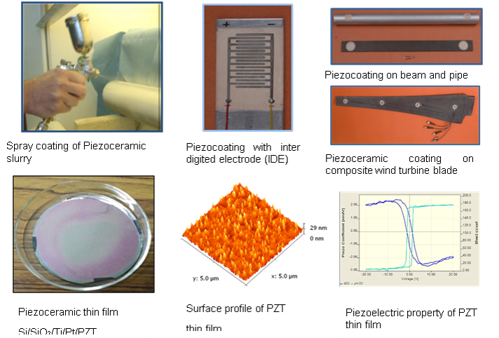
Application specific processes and materials have been developed for Piezoceramic thin films and coatings covering the thickness range 200 nm to 500 µm on various substrates (metal, composite and polymer). There are different techniques developed for the coating to specifically achieve the thickness of 200 nm to 600 nm, 1 µm to 40 µm and above 40 µm. Piezoceramic coating of 40 µm to 500 µm has been developed by spraying a flowable slurry in a distributed or continuous manner using hand held equipments. The developed Piezoceramic coating combines the features of bulk piezo ceramic and flexible piezo polymer. This coating has undergone stringent tests and found to be suitable for field applications. Direct bonding to the test object enhances its performance by reducing the transduction losses. This coating has been successfully tested for local and global Structural Health Monitoring (SHM) as transceiver of acousto ultrasonic waves.
Piezoceramic thin films in the thickness range 200 nm to few µm has been especially developed on Si/SiO2/Ti/Pt wafer for MEMS and microsensor applications using RF sputtering and Spin coating methods. In the low dimensional range 200 nm to 1 µm, substantial enhancement in the Piezoelectric property is achieved through directional growth and domain engineering by indigenous process optimization.


 English
 हिन्दी