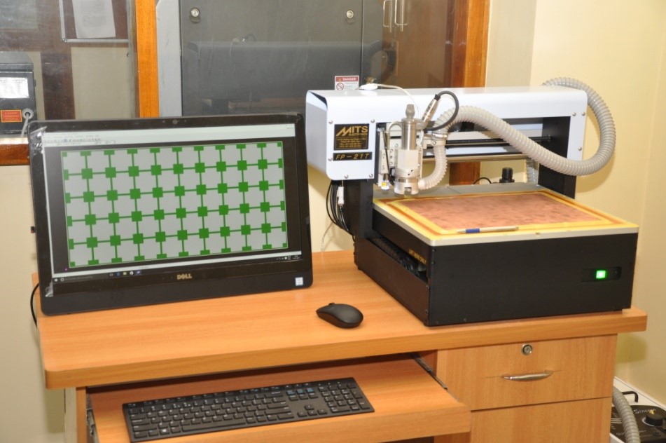
This state-of-the-art facility was established at CEM, CSIR-NAL in 2017. PCB prototyping machine is capable of milling, drilling, and routing the PCB laminates as per given Gerber/ DXF file. The salient features of the facility are;
Working area of machine: 350 mm x 250 mm
Milling resolution: 0.2 mm
Capable of milling double layered PCB
Year of Establishment
2017
Test Applications
The facility is fit for the fabrication of antenna, FSS, and metasurface structures.
Electronic circuit on PCB
Image