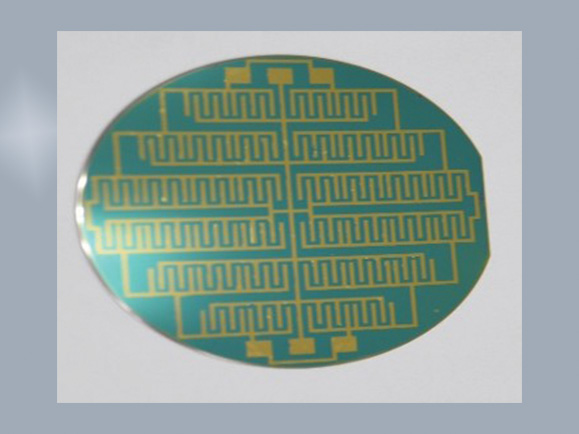
Prototyping of PZT and BST thin films (~350nm-1000nm) on SOI (Silicon on Insulator) with stack design SOI/Ti/Pt/PZT and SOI/Ti/Pt/BST, called MEMS chip, having roughness ~2nm for the development of MEMS transducers for aerospace and defence applications.
Year of Development
2022-2025
Salient Technical Features
A wafer-scale (φ=4‘’) Piezo MEMS chip engineered for high-efficiency ultrasonic transducer systems offers advanced microfabrication precision, exceptional sensitivity, and seamless integration into array architectures via advanced microfabrication, delivering ultra-compact, low-power, and high-bandwidth multifunctional microsystems for precision sensing and intelligent control applications.
Level/Scale of Development
TRL=6 Qualified MEMS chip for product development
Applications
• Ultrasonic transducer for underwater imaging application for defence purposes • Dynamic pressure sensor (1-5 bar) • Non-destructive testing and industrial inspection • Precision acoustic sensors and actuators • Medical diagnostics and therapeutic ultrasound devices
Commercialization
Technology is ready for commercialisation
Available in Market
Not available in Indian market. Piezo wafers are imported
Image